- Original research
- Open access
- Published:
Suppression strategy for the inrush current of a solid-state transformer caused by the reclosing process
Protection and Control of Modern Power Systems volume 8, Article number: 53 (2023)
Abstract
The automatic reclosing strategy is an effective measure to improve the reliability of a distribution network. It can quickly clear instantaneous faults in the grid. The traditional transformer has proven to be reliable and robust during the reclosing process. However, the influence of the reclosing process on the operational characteristics and reliability of solid-state transformers (SST) is still unclear. The reclosing action may generate a huge inrush current, resulting in shutdown and even damage of the SST. To address this problem, this paper proposes an inrush current suppression strategy. First, the operational performance of the SST under a reclosing process is discussed, and the inrush current generation mechanism is analyzed in detail. Then, considering the controllability of distributed generation (DG), a novel DG-supported inrush current suppression strategy is proposed. The suppression ability of the DG on inrush current in different initial conditions is analyzed. Finally, the effectiveness of the proposed strategy is verified by simulation and experiment. These show that the proposed strategy can help to enhance the FRT capability of the SST, as well as support the SST to maintain continuous power supply and physical integrity during grid faults.
1 Introduction
The extensive use of distributed energy resources (DER) and energy storage (ES) systems has promoted the modernization of the distribution network but also complicated power flow management at the distribution level [1]. Compared with traditional transformers that enable only simple functions such as voltage level scaling and electrical isolation, a solid-state transformer (SST) provides an excellent solution for managing power flow and information exchange between various micro sources, loads, and utility grids [2,3,4]. In addition, SST has also been equipped with other additional capabilities such as full-range control of terminal voltage and current [5, 6], power quality adjustment [7], providing DC ports [8], and FRT [9]. Therefore, SST is expected to be a key element in modern power distribution systems [10].
Resilience to unexpected events is one of the core objectives of modern distribution systems. Therefore, transformers are required to ride-through grid faults. Traditional low-frequency magnetic transformers have proven to be highly reliable and robust, and thus possess an inherent ability for FRT. However, the FRT capability of an SST is an unresolved issue because of the general performance restriction of power electronic equipment [11, 12]. On the one hand, in the event of grid faults, an SST is required to maintain grid-connection and provide reactive support to facilitate voltage restoration for a certain period of time so as to ride-through temporary faults as far as possible [12]. On the other hand, because of the weak robustness and tolerance of the semiconductor devices used in SST, transient overcurrent and large short-circuit current that may occur during grid faults can easily lead to the destruction of the SST [13]. Therefore, the SST may face serious challenges in terms of continuous power supply and physical integrity during unexpected events, especially grid faults.
In terms of power supply continuity, some research has been conducted on the operating characteristics and regulation strategies of an SST in DC grid fault conditions [9, 14,15,16,17], and AC grid fault conditions [18,19,20,21,22]. In the case of DC faults, the short-circuit fault current needs to be interrupted or limited by active methods because of the lack of natural current zero crossing. Traditional methods of handling DC faults rely on AC or DC circuit breakers (CB). However, all kinds of CBs, including mechanical CBs [23], solid-state CBs [24], and hybrid CBs [25], do not yet offer a good combination of characteristics in terms of response speed, cost, efficiency, and size. To avoid the use of CBs, references [9, 14,15,16,17] use the fact that the active management and clearing of a DC fault relies on the fast current control capability of the SST. This is an attractive FRT solution, which avoids the additional cost and footprint caused by CBs while enabling fast response. The case of an AC grid fault may have a much wider impact because the AC grid is usually the main power source of the SST [18]. Preliminary studies have been conducted for different fault types. For symmetric and asymmetric voltage sag conditions, reference [18] proposes an LVRT strategy that is suitable for bidirectional power transmission. When connected with new energy sources, some phases of the SST may inversely absorb active power during the LVRT and thus result in system overvoltage. The mechanism and suppression method of active power backflow during an LVRT are studied in [19]. For single-phase-to-neutral fault conditions, the operational mode of an SST can be switched from three-phase to two-phase to minimize the outage area. The steady-state performance and transient performance during the two-phase operation are studied respectively in [20] and [21, 22], respectively. In summary, with proper control, an SST is able to continuously supply power to end-users in the event of DC and AC grid faults.
On the other hand, ensuring the physical integrity of an SST during operation is another challenge. This issue has not received much attention. Compared with traditional transformers, SSTs have a much lower tolerance to overvoltage and overcurrent, which greatly affects their reliability and application [26]. Reference [27] designs a novel soft-start procedure for an SST to limit the inrush current and avoid overcurrent during the startup process. To limit the inrush current deriving from the transition in the case of a power module failure, reference [28] proposes a novel redundancy scheme for an SST that can accomplish the faulty power module replacement process with nearly no transition. Ensuring that SSTs are protected from damage during onset and grid faults will be more challenging because of the potential of high overcurrent [29]. To address this problem, existing studies have proposed corresponding overcurrent protection strategies from both hardware and software perspectives [30]. On the hardware side, series converters [31] and fault current limiters [32, 33] can be used to limit persistent overcurrent during voltage dips, whereas hysteresis compensators [34] can suppress inrush current when faults occur. However, these devices will increase system cost while they do not supply a grid support function. Compared to the hardware-based, software-based approaches enable device protection at a lower cost by flexibly modifying the control strategy [35,36,37] or regulating the current reference value [38,39,40,41]. However, most existing literature focuses on the SST devices themselves, while ignoring the dynamic interactions among the devices in the distribution network. In addition, there are also few studies on the self-protection and continuous power supply of an SST during grid faults by flexibly dispatching multiple available resources in the distribution system.
The instantaneous fault is the most common fault type in distribution networks. Its occurrence rate is far higher than that of the permanent fault. To deal with the instantaneous fault and improve power supply reliability, automatic-reclosing strategies have been widely used. That is, the circuit breaker will trip immediately to cut off the power supply when a grid fault occurs and then reclose automatically after a predetermined period of time. For an instantaneous fault, the fault has been cleared so the circuit breaker recloses to restore the power supply. On the contrary, for a permanent fault, the circuit breaker will trip again and no further reclosing is activated. Traditional transformers have been proven to be reliable and robust in the process of reclosing after long-term optimization. However, the operational characteristics and reliability of SSTs during the reclosing process are still unclear.
This paper studies the operational characteristics and control methods of an SST in the process of reclosing to support its safe and reliable ride-through operation of grid faults. In Sect. 2, the circuit topology and control strategy of the SST are briefly reviewed, and the operational performance of the SST in the reclosing process is discussed. In Sect. 3, the generation mechanism of inrush current during the reclosing process is analyzed in detail. In Sect. 4, considering the controllability of distributed generation (DG), a novel DG-supported inrush current suppression strategy is proposed, and the suppression ability of a DG on inrush current under different initial conditions is analyzed. Finally, in Sect. 5 simulation and experimental results are provided to validate the theoretical analysis and control methods.
2 Operating characteristics of the SST during the reclosing process
2.1 Review of the SST
A typical three-stage SST consists of a medium-voltage (MV) input stage, an isolation stage, and a low-voltage (LV) output stage [42]. The input stage uses a cascaded H-bridge (CHB) converter to interact at the MV level with the AC grid and create a MV DC bus (MDCB). The isolation stage adopts the isolated dual-active-bridge (IDAB) converter to isolate disturbances and form a low-voltage DC bus (LDCB). The LV output stage is composed of a three-phase four-wire converter to form an LV AC grid and interact with the LDCB. The MV DC and LV DC are available for connecting DGs and ESs. The overall architecture of the studied SST is shown in Fig. 1. As shown, eabc is the phase voltage of the MV AC grid, iabc is the phase current absorbed from the AC grid, u(abc)N is the input voltage of the CHB, while v(abc)Hi and i(abc)Hi (i = 1,2,…,n) are the output DC voltage and input AC current of each CHB submodule.

Overall topology of the studied SST
Typically, each stage of the SST is controlled by its local controllers and is used to achieve different control objectives. In the CHB control, the outer MV DC controller regulates the DC-link capacitor voltage, and the inner current controller tracks the desired current reference. The control strategy is shown in Fig. 2, where vH-ref are the reference values of v(abc)Hi (i = 1,2,…,n), and vsum is the sum of the DC voltages of all CHB submodules, i.e.:

Control block diagram of the input stage of SST
The IDAB is designed to regulate the constant voltage of the LDCB and the power balance between DC/DC converter cells, as shown in Fig. 3. The control of the input-side and output-side DC voltages is achieved by adjusting the phase shift duty cycle of the IDAB.

Control block diagram of the isolation stage of SST
2.2 Operating characteristic of SST in the traditional control strategy during the reclosing process
A typical distribution system with an SST is shown in Fig. 4. As seen, the SST is connected at the end of the distribution network to manage the DER and ES systems. The output power of the SST is PO, and the power absorbed by the load and that generated by the DG are Pload and PDG, respectively. The automatic reclosing device is equipped with a breaker (QF3). For 35 kV and 10 kV systems, the reclosing acceleration strategy is generally adopted to quickly remove instantaneous faults. QF4 and QF5 control the load and DG, respectively.

System structure of the distribution system
The sequence of the reclosing process is shown in Fig. 5. At time t0, the grid fault occurs at point A or B. Then the relay protection acts, and the breaker QF3 is opened at time t1. At t2, the automatic reclosing strategy operates, and QF3 is reclosed. The time interval between t1 and t2 is usually 1 s. The voltage and current waveforms during the reclosing process are shown in Fig. 6.

The time sequence of the reclosing process

Voltage and current waveforms of the SST during the reclosing process
As shown in Fig. 6, the three-phase input current of the SST drops to 0 immediately when the breaker QF3 is opened at 0.4 s. The MDCB voltage and LDCB voltage immediately begin to drop one after another, and down to 0 within 0.15 s when no load rejection is implemented.
When the circuit breaker recloses at 1.4 s, both the MDCB and LDCB voltages increase immediately. At the same time, the input current also rises rapidly and far exceeds the rated current. Such a large inrush current would trigger the SST's protection system.
3 Generation mechanism and influencing factors of the inrush current
3.1 Generation mechanism of the inrush current during the reclosing process
From the topology of the SST input stage shown in Fig. 1, the state equation of phase A of the CHB can be expressed as:
where Sai is the switching function of the ith module of phase a, and R is the parasitic resistance of L. The neutral point to ground voltage is expressed as uNO, which is 0 in symmetric power systems. uNO and uaN can be calculated as:
Other physical quantities are defined in Fig. 1, while the state equations of other phases can be written according to that of phase A.
In the dq frame, Eq. (1) can be rewritten as:
where edq, idq, and udq are the components of eabc, iabc, and uabc on the d- and q-axes, respectively, while ω is the fundamental frequency.
PI controllers are adopted in the MV DC voltage controller and the current controller, as:
where idq* is the reference value of idq, KvP and KvI are the proportional and integral coefficients of the DC voltage controller, respectively, while KiP and KiI are the corresponding proportional and integral coefficients of the current controller.
Substituting (3) into (2) yields:
Thus the change rate of id can be obtained from (4), as:
When the breaker closes again, there is a large deviation between the expected value and the measured value of the DC side voltage, i.e., 3nvH-ref and vsum. The large deviation further leads to a large d-axis current reference \(i_{d}^{*}\) according to (3) and a large change rate of d-axis current according to (5). Therefore, the inrush current will appear and reach its extreme value when the change rate of the d-axis current is 0. The maximum inrush current id-max can be calculated by:
As can be seen from (6), the closer the actual and reference values of the MDCB voltage, the smaller the inrush current.
3.2 Influence of the initial phase angle on the inrush current
The effect of the voltage phase on the inrush current is analyzed in this subsection. Phase A is again taken as an example, and its equivalent circuit is shown in Fig. 7. From Fig. 7, the circuit equation can be obtained as:
where

Equivalent circuit of phase A
We take the fundamental components of voltage for analysis. They are given as:
where θ and φ are the initial phase angles of ea and ua, and Em and Um are the voltage amplitudes of ea and ua, respectively.
According to (9) and (7), there is
where
At the moment of reclosing action, ia is 0. Solving the differential equation in (10) yields:
where
and
Similarly, the start-up currents of phases B and C can be obtained. As shown in (13), the inrush current is related to the angle γ–α. Therefore, adjusting the initial angle is a way to reduce the inrush current.
In terms of a three-phase system, the inrush currents of the three phases are difficult to optimize by phase-angle control simultaneously. Therefore, DC voltage stability control will be mainly considered in the simulations and experiments below.
4 Proposed inrush current suppression strategy
4.1 Regulation range of DG output power to inrush current
Stabilizing the DC voltage of the SST around its reference value helps to suppress the inrush current. To achieve this goal, an external power supply is required to provide energy support for the DC capacitor. It is worth noting that the SST is mainly used to manage the DGs and ES systems of an AC/DC hybrid microgrid, rather than simply replacing the traditional transformer, as shown in Fig. 8. This provides a new solution for the FRT of SST, that is, suppressing the inrush current by reasonably scheduling the energy in the DGs and ES systems. In order to simplify the analysis, the DGs and ES systems connected to the microgrid will be considered as a whole.

Diagram of SST for microgrid energy management
We assume that the output power of the DG is adjusted at the time tS, and that the adjustment must be started before the MDCB voltage drops to 0 to ensure the stability of the LDCB voltage. Then the time sequence of the reclosing process shown in Fig. 5 can be modified as shown in Fig. 9, where Δt is the time interval from QF3 disconnection to MDCB voltage dropping to 0. Then there is:
where CH is the input side DC link capacitance, and
where PO, Pload and PDG have been defined in Fig. 4.

Time sequence of reclosing process considering DG operation
Generally, DGs in the AC/DC microgrid are in their maximum output state, while the power output PO of the SST is small. In addition, DGs are usually controlled by power electronic devices and can respond quickly. Therefore, the DG power can be adjusted in time before the MDCB voltage drops to 0.
At the moment of circuit breaker opening, i.e., t1, the DG output power PDG⟨t1⟩ may be larger or lower than the load demand power Pload⟨t1⟩. An analysis of the two conditions is provided in the following paragraphs.
-
(1)
PDG⟨t1⟩ ≥ Pload⟨t1⟩
Between moments t1 and tS, the energy generated by the DG cannot be fully consumed by the load, and the excess energy will be stored in the input side DC link capacitor. This will raise the MDCB voltage, and there is:
$$\mu P_{{\text{O}}} \left\langle {t_{1} } \right\rangle \times \left( {t_{{\text{S}}} { - }t_{1} } \right) = \frac{1}{2}C_{{\text{H}}} \sum\limits_{{j = {\text{a}},{\text{b}},{\text{c}}}} {\sum\limits_{i = 1}^{n} {\left( {v_{{\text{H}}}^{2} \left\langle {t_{1} } \right\rangle - v_{{j{\text{H}}i}}^{2} \left\langle {t_{{\text{S}}} } \right\rangle } \right)} }$$(15)where μ is the transmission efficiency of the DAB. At time tS, the DG reduces its output power and makes it less than the load power demand. Therefore, the surplus energy of the input side DC link capacitor will be consumed, and then:
$$P_{{\text{O}}} \left\langle {t_{{\text{S}}} } \right\rangle \times \left( {t_{2} - t_{{\text{S}}} } \right) = \frac{\mu }{2}C_{{\text{H}}} \sum\limits_{{j = {\text{a}},{\text{b}},{\text{c}}}} {\sum\limits_{i = 1}^{n} {\left( {v_{{j{\text{H}}i}}^{2} \left\langle {t_{{\text{S}}} } \right\rangle - v_{{j{\text{H}}i}}^{2} \left\langle {t_{2} } \right\rangle } \right)} }$$(16)where
$$\left\{ {\begin{array}{*{20}l} {P_{{\text{O}}} \left\langle {t_{{\text{S}}} } \right\rangle = P_{{{\text{load}}}} \left\langle {t_{{\text{S}}} } \right\rangle - P_{{{\text{DG}}}} \left\langle {t_{{\text{S}}} } \right\rangle } \hfill \\ {P_{{{\text{load}}}} \left\langle {t_{{\text{S}}} } \right\rangle = P_{{{\text{load}}}} \left\langle {t_{1} } \right\rangle } \hfill \\ \end{array} } \right.$$According to (15) and (16), the output power of the DG at time tS can be adjusted as:
$$\begin{aligned} P_{{{\text{DG}}}} \left\langle {t_{{\text{S}}} } \right\rangle = & \frac{{\mu C_{{\text{H}}} \sum\limits_{{j = {\text{a}},{\text{b}},{\text{c}}}} {\sum\limits_{i = 1}^{n} {\left( {v_{{j{\text{H}}i}}^{2} \left\langle {t_{{2}} } \right\rangle - v_{{\text{H - ref}}}^{2} } \right)} } }}{{2(t_{2} - t_{{\text{S}}} )}} \\ & + \frac{{\mu^{2} \left( {P_{{{\text{load}}}} \left\langle {t_{1} } \right\rangle - P_{{{\text{DG}}}} \left\langle {t_{1} } \right\rangle } \right)\left( {t_{{\text{S}}} - t_{1} } \right)}}{{\left( {t_{2} - t_{{\text{S}}} } \right)}} + P_{{{\text{load}}}} \left\langle {t_{{\text{S}}} } \right\rangle \\ \end{aligned}$$(17)
-
(2)
PDG⟨t1⟩ < Pload⟨t1⟩
Before the DG adjusts its output power, the input side DC link capacitor will provide energy to the load. Therefore, the input DC link voltage will drop, as:
$$P_{{\text{O}}} \left\langle {t_{{\text{S}}} } \right\rangle \times \left( {t_{{\text{S}}} - t_{1} } \right) = \frac{\mu }{2}C_{{\text{H}}} \sum\limits_{{j = {\text{a}},{\text{b}},{\text{c}}}} {\sum\limits_{i = 1}^{n} {\left( {v_{{\text{H - ref}}}^{2} - v_{{j{\text{H}}i}}^{2} \left\langle {t_{{\text{S}}} } \right\rangle } \right)} }$$(18)At time tS, it is necessary to cut off the load and the energy output by the DG is used to compensate for the energy deficiency in the input side DC link capacitor, thus:
$$\mu P_{{\text{O}}} \left\langle {t_{{\text{S}}} } \right\rangle \left( {t_{2} - t_{{\text{S}}} } \right) = \frac{{1}}{2}C_{{\text{H}}} \sum\limits_{{j = {\text{a}},{\text{b}},{\text{c}}}} {\sum\limits_{i = 1}^{n} {\left( {v_{{j{\text{H}}i}}^{2} \left\langle {t_{{\text{S}}} } \right\rangle - v_{{j{\text{H}}i}}^{2} \left\langle {t_{2} } \right\rangle } \right)} }$$(19)where
$$\left\{ {\begin{array}{*{20}l} {P_{{\text{O}}} \left\langle {t_{{\text{S}}} } \right\rangle = P_{{{\text{load}}}} \left\langle {t_{{\text{S}}} } \right\rangle - P_{{{\text{DG}}}} \left\langle {t_{{\text{S}}} } \right\rangle } \hfill \\ {P_{{{\text{load}}}} \left\langle {t_{{\text{S}}} } \right\rangle = {0}} \hfill \\ \end{array} } \right.$$From (18) and (19), the output power of the DG at time tS can be adjusted as:
$$\begin{aligned} P_{{{\text{DG}}}} \left\langle {t_{{\text{S}}} } \right\rangle = & \frac{{C_{{\text{H}}} \sum\limits_{{j = {\text{a}},{\text{b}},{\text{c}}}} {\sum\limits_{i = 1}^{n} {\left( {v_{{j{\text{H}}i}}^{2} \left\langle {t_{2} } \right\rangle - v_{{\text{H - ref}}}^{2} } \right)} } }}{{2\mu \left( {t_{2} - t_{{\text{S}}} } \right)}} \\ & + \frac{{\left( {P_{{{\text{load}}}} \left\langle {t_{1} } \right\rangle - P_{{{\text{load}}}} \left\langle {t_{1} } \right\rangle } \right)\left( {t_{{\text{S}}} - t_{1} } \right)}}{{\mu^{2} \left( {t_{2} - t_{{\text{S}}} } \right)}} \\ \end{aligned}$$(20)To ensure that the inrush current generated by the SST does not cause the circuit breaker to operate incorrectly when the reclosing operation is performed, the inrush current shall be less than 1.2–1.3 times of the rated current, i.e.:
$$\left| {i_{{\text{d - max}}} } \right| < k\left| {i_{{{\text{dN}}}} } \right|,k \in \left[ {1.2,1.3} \right]$$(21)Substituting (21) into (6) obtains:
$$\left| {3nv_{{\text{H - ref}}} - v_{{{\text{Hsum}}}} } \right| < k\frac{{R + K_{{{\text{iP}}}} }}{{K_{{{\text{iP}}}} K_{{{\text{vP}}}} }}\left| {i_{{{\text{dN}}}} } \right|$$(22)From (17), (20), and (22), the compensation power of DG can be obtained as:
$$P_{{{\text{DG}}}} \left\langle {t_{{\text{S}}} } \right\rangle = \left\{ {\begin{array}{*{20}l} {\frac{{\mu \left( {K_{1} + \mu^{2} K_{2} } \right)}}{{t_{2} - t_{{\text{S}}} }} + P_{{{\text{load}}}} \left\langle {t_{{\text{S}}} } \right\rangle } \hfill & {,P_{DG} \left\langle {t_{1} } \right\rangle \ge P_{{{\text{load}}}} \left\langle {t_{1} } \right\rangle } \hfill \\ {\frac{{K_{1} + K_{2} }}{{\mu (t_{2} - t_{{\text{S}}} )}}} \hfill & {,P_{DG} \left\langle {t_{1} } \right\rangle < P_{{{\text{load}}}} \left\langle {t_{1} } \right\rangle } \hfill \\ \end{array} } \right.$$(23)where
$$\left\{ \begin{gathered} K_{1} = \frac{{3nC_{{\text{H}}} \left( {v_{{\text{H}}}^{\prime 2} (t_{{2}} ) - v_{{\text{H - ref}}}^{2} } \right)}}{2} \hfill \\ K_{2} = \frac{{\left( {P_{{{\text{load}}}} \left\langle {t_{1} } \right\rangle - P_{{{\text{DG}}}} \left\langle {t_{1} } \right\rangle } \right)\left( {t_{{\text{S}}} - t_{1} } \right)}}{\mu } \hfill \\ \end{gathered} \right.$$where the range of the MDCB voltage when the circuit breaker is closed is expressed as v’H(t2) and shall be:
$$v_{{\text{H}}}^{\prime } \left\langle {t_{2} } \right\rangle \in \left[ {v_{{\text{H - ref}}} - \frac{k}{3n}\frac{{R + K_{{{\text{iP}}}} }}{{K_{{{\text{iP}}}} K_{{{\text{vP}}}} }}\left| {i_{{{\text{dN}}}} } \right|,\;v_{{\text{H - ref}}} + \frac{k}{3n}\frac{{R + K_{{{\text{iP}}}} }}{{K_{{{\text{iP}}}} K_{{{\text{vP}}}} }}\left| {i_{{{\text{dN}}}} } \right|} \right]$$(24)
4.2 DG-supported inrush current suppression strategy
To reduce the inrush current, the energy in the input side DC link capacitor should be regulated in time to control the capacitor voltage before the circuit breaker recloses. Based on this, a novel DG-supported inrush current suppression strategy is proposed as shown in Fig. 10.

The DG-supported inrush current suppression strategy
From (23) and (24), the feasible region of impulse current suppression strategy can be obtained, as shown in Fig. 11 and given as:

Feasible domain of the proposed strategy
-
(1)
Strategy A: PDG⟨t1⟩ ≥ Pload⟨t1⟩
After QF3 trips, the MDCB voltage rises gradually, while the LDCB voltage remains stable and QF4 remains closed. At this time, after the DG response, it is necessary to consume the excess energy in the input side DC link capacitor through the load. Therefore the DG adjusts its output power as:
$$\begin{gathered} P_{{{\text{DG}}}} \left\langle {t_{{\text{S}}} } \right\rangle = \frac{{3n\mu C_{{\text{H}}} \left( {v_{{\text{H}}}^{\prime 2} \left\langle {t_{2} } \right\rangle - v_{{\text{H - ref}}}^{2} } \right)}}{{2\left( {t_{2} - t_{{\text{S}}} } \right)}} + P_{{{\text{load}}}} \left\langle {t_{{\text{S}}} } \right\rangle \hfill \\ + \frac{{\mu^{2} \left( {P_{{{\text{load}}}} \left\langle {t_{1} } \right\rangle - P_{{{\text{DG}}}} \left\langle {t_{1} } \right\rangle } \right)\left( {t_{{\text{S}}} - t_{1} } \right)}}{{\left( {t_{2} - t_{{\text{S}}} } \right)}} \hfill \\ \end{gathered}$$(26)
-
(2)
Strategy B: PDG⟨t1⟩ < Pload⟨t1⟩
After QF3 trips, the MDCB voltage drops gradually, while the LDCB voltage remains stable. Since the DG power supply cannot meet the load demand, it is necessary to trip the load, i.e., QF4 is disconnected. At this time, after the DG response, it is necessary to compensate for the energy required for the input side DC link capacitor before reclosing the circuit breaker. Therefore, the required DG power is:
$$\begin{aligned} P_{{{\text{DG}}}} \left\langle {t_{{\text{S}}} } \right\rangle & = \frac{{3nC_{{\text{H}}} \left( {v_{{\text{H}}}^{\prime 2} \left\langle {t_{2} } \right\rangle - v_{{\text{H - ref}}}^{2} } \right)}}{{2\mu \left( {t_{2} - t_{{\text{S}}} } \right)}} \\ & \quad + \frac{{\left( {P_{{{\text{load}}}} \left\langle {t_{1} } \right\rangle - P_{{{\text{DG}}}} \left\langle {t_{1} } \right\rangle } \right)\left( {t_{{\text{S}}} - t_{1} } \right)}}{{\mu^{2} \left( {t_{2} - t_{{\text{S}}} } \right)}} \\ \end{aligned}$$(27)
5 Simulation and experimental results
5.1 Simulation Results
To verify the effectiveness of the proposed inrush current suppression method, a MATLAB/Simulink simulation model containing a DG, an SST and load is established. The system simulation parameters are shown in Table 1.
From (14) and (21), after the circuit breaker is opened, the minimum time for the MDCB voltage to drop to 0 is:
and the rated current value is:
where ES and IN are the amplitudes of the grid voltage and rated current, respectively.
When the circuit breaker is reclosed, then from (21), to keep the inrush current less than 1.3 times the rated current, the operating range of the MDCB voltage shall be:
-
(1)
Mode I: PDG⟨t1⟩ = 500 kW ≥ Pload⟨t1⟩ = 400 kW.
The circuit breaker opens at 0.4 s and recloses at 1.4 s. Between 0.4 s and 0.5 s, the input side DC link capacitor is in a charge state, and its voltage gradually increases. It is assumed that the output power of the DG is adjusted to 400 kW at 0.5 s. In this case, if the traditional control strategy is adopted, the inrush current will be greater than 1.3In, as shown in Fig. 12.
Fig. 12 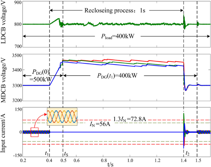
DC bus voltage and input current waveforms with traditional control strategy (Mode I)
From (23), to limit the inrush current, the power adjustment range of the DG shall be:
$$386.1\;{\text{kW}} \le P_{{{\text{DG}}}} \left( {t_{{\text{S}}} } \right) \le 394.9\;{\text{kW}}$$Based on this, the output power of the DG is adjusted to 386.1 kW, and the new voltage and current waveforms are shown in Fig. 13. As seen there, the inrush current is less than 1.3In, and the SST can remain operational.
Fig. 13 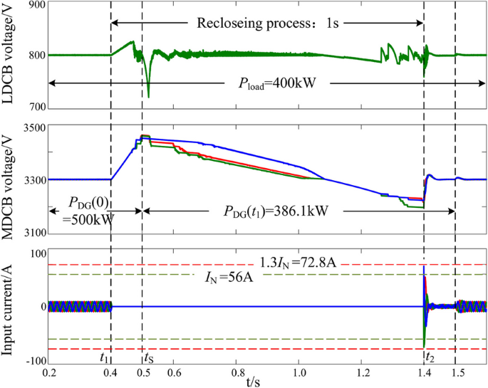
DC bus voltage and input current waveforms with proposed strategy (Mode I)


-
(2)
Mode II: PDG⟨t1⟩ = 300 kW < Pload⟨t1⟩ = 400 kW.
The circuit breaker opens at 0.4 s and recloses at 1.4 s. Between 0.4 s and 0.5 s, the input side DC link capacitor is in a discharge state, and its voltage gradually decreases. At 0.5 s, the load needs to be disconnected because the DG power supply cannot fully provide the power required by the load. It is assumed that the output power of the DG is adjusted to 0 at 0.5 s, and consequently the MDCB voltage cannot reach its reference value. In this case, if the traditional control strategy is adopted, the inrush current will be greater than 1.3In, as shown in Fig. 14.
Fig. 14 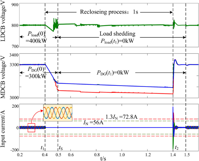
DC bus voltage and input current waveforms with traditional control strategy (Mode II)
From (23), to limit the inrush current, the power adjustment range of the DG shall be:
$$7.3\;{\text{kW}} \le P_{{{\text{DG}}}} \left( {t_{{\text{S}}} } \right) \le 18.6\;{\text{kW}}$$Based on this, the output power of the DG is adjusted to 18.6 kW, and the new voltage and current waveforms are shown in Fig. 15. It can be seen that the inrush current is less than 1.3In, and the SST can remain in operation.
Fig. 15 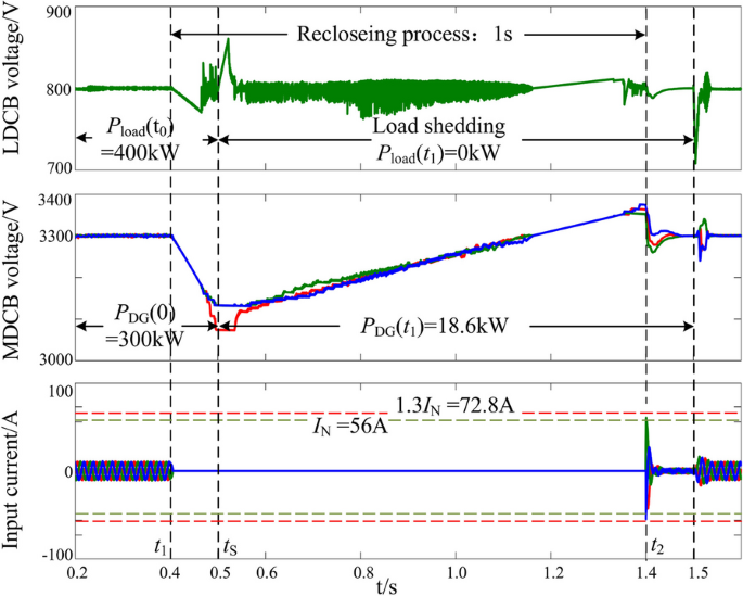
DC bus voltage and input current waveforms with proposed strategy (Mode II)
Comparing Figs. 12, 13, 14 and 15, it can be seen that the inrush current can be limited to the expected range by adjusting the output power of the DG.


5.2 Experimental results
Low-voltage experiments are carried out to further verify the correctness and effectiveness of the suppression strategy proposed. The experimental parameters are listed in Table 2 and the experiments are conducted in two conditions.
(1) Mode I: PDG⟨t1⟩ = 4 kW ≥ Pload⟨t1⟩ = 3 kW.
The corresponding experimental results are shown in Fig. 16.

DC bus voltage and input current waveforms in mode I
(i) The SST works under the traditional control strategy. At time t1, the circuit breaker is opened, and the MDCB voltage increases to 510 V. At time tS, the SST suspends the energy exchange between the DG and load. Then the MDCB voltage remains constant. At time t2, the circuit breaker is reclosed. The MDCB voltage falls to the pre-set value instantaneously, and a large inrush current appears on the AC side.
(ii) The SST works under the proposed control strategy. At time t1, the circuit breaker is opened, and the MDCB voltage increases to 510 V. At time tS, the output power of the DG is adjusted and the MDCB voltage begins to decrease. At time t2, the circuit breaker is reclosed, and the inrush current is less than 1.3 times the rated current.
(2) Mode II: PDG⟨t1⟩ = 2 kW < Pload⟨t1⟩ = 3 kW.
The corresponding experimental results are shown in Fig. 17.
-
(i)
The SST works under the traditional control strategy. At time t1, the circuit breaker is opened, and the MDCB voltage decreases to 485 V. At time t2, the circuit breaker is reclosed. The MDCB voltage increases to the pre-set value instantaneously, and a large inrush current appears on the AC side.
-
(ii)
The SST works under the proposed control strategy. At time t1, the circuit breaker is opened, and the MDCB voltage decreases to 490 V. At time tS, the output power of the DG is adjusted and the MDCB voltage begins to increase. At time t2, the circuit breaker is reclosed, and the inrush current is close to 1.3 times of the rated current.

DC bus voltage and input current waveforms in mode II
To further reduce the inrush current, the output power of the DG can be calculated based on Sect. 3. The experimental waveforms are shown in Fig. 18. During the reclosing process, the MDCB voltage can be controlled within a reasonable range, and there is no inrush current on the AC side.

DC bus voltage and input current waveforms while inrush current is 0
In summary, the inrush current suppression strategy proposed in this paper can guarantee the stability of the output side DC bus and suppress the inrush current generated during the reclosing process.
6 Conclusion
In this paper, the SST inrush current caused by the reclosing process after power grid faults is analyzed, and a new DG-based inrush current suppression strategy is proposed. The proposed strategy helps to enhance the FRT capability of the SST and supports the SST in maintaining continuous power supply and physical integrity during grid faults. The main conclusions are as follows:
-
(1)
The internal mechanism of the SST inrush current caused by the reclosing process is analyzed. The reclosing action makes the instantaneous value of the SST DC side voltage deviate too much from its reference value, resulting in overshoots during the dynamic regulation process.
-
(2)
A new DG-based inrush current suppression strategy is proposed. This strategy provides short-term energy support for the SST by reasonably scheduling the energy in DGs, so as to stabilize the DC voltage of the SST. This further limits the error between the actual DC voltage and its reference value to a certain range to suppress the inrush current and achieve reliable FRT.
-
(3)
The suppression ability of the DG on inrush current, i.e., the adjustable power range of the DG, in different initial conditions is analyzed. It shows that the energy supply relationship between the DG and load should be fully considered, and different control strategies should be adopted for different operating conditions.
It is worth noting that in practical engineering application, the proposed control strategy may be limited by the capacity of new energy sources, and therefore cannot achieve suppression of SST inrush current under all operating conditions. However, this paper proposes a generalized approach and solution to maintain the power supply continuity and physical integrity of an SST during grid faults by rationally scheduling flexible resources in distribution networks.
Availability of data and materials
Not applicable.
Abbreviations
- CB:
-
Circuit breakers
- CHB:
-
Cascaded H-bridge
- DER:
-
Distributed energy resource
- DG:
-
Distribution generation
- ES:
-
Energy storage
- FRT:
-
Fault ride-through
- IDAB:
-
Isolated dual active bridge
- LDCB:
-
Low-voltage DC bus
- LV:
-
Low-voltage (LV)
- MDCB:
-
Medium-voltage DC bus
- MV:
-
Medium-voltage
- SST:
-
Solid state transformer
References
Ruiz, F., Perez, M. A., Espinosa, J. R., Gajowik, T., Stynski, S., & Malinowski, M. (2020). Surveying solid-state transformer structures and controls: Providing highly efficient and controllable power flow in distribution grids. IEEE Industrial Electronics Magazine, 14(1), 56–70.
Huang, A. Q., Crow, M. L., Heydt, G. T., Zheng, J. P., & Dale, S. J. (2010). The future renewable electric energy delivery and management (freedm) system: The energy internet. Proceedings of the IEEE, 99(1), 133–148.
Huang, K., Li, Y., Zhang, X., Liu, L., Zhu, Y., & Meng, X. (2021). Research on power control strategy of household-level electric power router based on hybrid energy storage droop control. Protection and Control of Modern Power Systems, 6(1), 1–13.
Guo, H., Ding, F., Ren, L., Xiao, Y., Wang, F., & Shi, T. (2023). Adaptive mode switching and power management of a solid-state transformer-based active distribution network (in Chinese). Power System Protection and Control, 3, 89–98.
Huber, J. E., & Kolar, J. W. (2017). Applicability of solid-state transformers in today’s and future distribution grids. IEEE Transactions on Smart Grid, 10(1), 317–326.
Wang, H., & Luan, J. (2020). Summary of power electronic evolution of transformer and its influence on voltage stability (in Chinese). Power System Protection and Control, 48(16), 171–192.
Gorla, N. B. Y., Kolluri, S., Chai, M., & Panda, S. K. (2018). A comprehensive harmonic analysis and control strategy for improved input power quality in a cascaded modular solid state transformer. IEEE Transactions on Power Electronics, 34(7), 6219–6232.
Tahir, Y., Khan, I., Rahman, S., Nadeem, M. F., Iqbal, A., Xu, Y., & Rafi, M. (2021). A state-of-the-art review on topologies and control techniques of solid-state transformers for electric vehicle extreme fast charging. IET Power Electronics, 14(9), 1560–1576.
Weng, H., Li, J., Shi, K., Chen, M., Krein, P.T., & Xu, D. (2021). A DC solid state transformer with dc fault ride-through capability. IEEE Journal of Emerging and Selected Topics in Power Electronics.
Mishra, D. K., Ghadi, M. J., Li, L., Hossain, M. J., Zhang, J., Ray, P. K., & Mohanty, A. (2021). A review on solid-state transformer: A breakthrough technology for future smart distribution grids. International Journal of Electrical Power & Energy Systems, 133, 107255.
Nadour, M., Essadki, A., & Nasser, T. (2020). Improving low-voltage ride-through capability of a multimegawatt dfig based wind turbine under grid faults. Protection and Control of Modern Power Systems, 5(1), 1–13.
Chen, L., Li, G., Chen, H., Ding, M., Zhang, X., Li, Y., Xu, Y., Ren, L., & Tang, Y. (2020). Investigation of a modified flux-coupling-type SFCL for low-voltage ride-through fulfillment of a virtual synchronous generator. IEEE Transactions on Applied Superconductivity, 30(4), 1–6.
Chen, L., Qiao, X., Zhao, Z., Wang, X., Chen, H., Li, Y., Islam, M. R., Deng, X., & Li, G. (2022). Coordination of mode switching control and smes unit for low-voltage ride-through fulfillment of power electronic transformer. Energy Science & Engineering, 10(3), 993–1008.
Zhang, J., Zhang, Y., Zhou, J., Wang, J., Shi, G., & Cai, X. (2022). Control of a hybrid modular solid-state transformer for uninterrupted power supply under MVDC short-circuit fault. IEEE Transactions on Industrial Electronics.
Li, R., Xu, L., Yao, L., & Williams, B. W. (2016). Active control of dc fault currents in dc solid-state transformers during ride-through operation of multi-terminal hvdc systems. IEEE Transactions on Energy Conversion, 31(4), 1336–1346.
Wang, T., Chu, X., Hussain, K. S. T., & Gao, J. (2022). Fault control and line protection strategy for lvdc microgrids based on modified high-frequency-link dc solid state transformer. International Journal of Electrical Power & Energy Systems, 140, 108052.
Ye, Y., Zhang, X., Jin, J., Wang, Y., & Yang, X. (2022). Analysis and design of a nonisolated dc transformer with fault current limiting capability. IEEE Transactions on Power Electronics, 37(8), 9876–9888.
Xiang, B., Luo, J., Gao, L., Liu, Z., Geng, Y., Wang, J., & Yanabu, S. (2020). Study on the parameter requirements for resistive-type superconducting fault current limiters combined with mechanical dc circuit breakers in hybrid ac/dc transmission grids. IEEE Transactions on Power Delivery, 35(6), 2865–2875.
Rodrigues, R., Du, Y., Antoniazzi, A., & Cairoli, P. (2020). A review of solid-state circuit breakers. IEEE Transactions on Power Electronics, 36(1), 364–377.
Han, X., Sima, W., Yang, M., Li, L., Yuan, T., & Si, Y. (2018). Transient characteristics under ground and short-circuit faults in a ±500 kv mmc-based hvdc system with hybrid dc circuit breakers. IEEE Transactions on Power Delivery, 33(3), 1378–1387.
Han, J., Kong, X., Li, P., Zhang, Z., & Yin, X. (2019). A novel low voltage ride through strategy for cascaded power electronic transformer. Protection and Control of Modern Power Systems, 4(1), 1–12.
Zhao, T., & Chen, D. (2021). Active power backflow control strategy for cascaded photovoltaic solid-state transformer during low-voltage ride through. IEEE Transactions on Industrial Electronics, 69(1), 440–451.
De Carne, G., Langwasser, M., Zhu, R., & Liserre, M. (2019). Smart transformer-based single phase-to-neutral fault management. IEEE Transactions on Power Delivery, 34(3), 1049–1059.
Zhu, R., & Liserre, M. (2019). Control of smart transformer under single-phase to ground fault condition. IEEE Transactions on Power Electronics, 35(2), 2034–2043.
Zhu, R., & Liserre, M. (2018). Continuous operation of smart transformer-fed distribution grid with single-phase faults. In 2018 IEEE Energy Conversion Congress and Exposition (ECCE) (pp. 458–464) IEEE.
Hannan, M. A., Ker, P. J., Lipu, M. S. H., Choi, Z. H., Rahman, M. S. A., Muttaqi, K. M., & Blaabjerg, F. (2020). State of the art of solid-state transformers: Advanced topologies, implementation issues, recent progress and improvements. IEEE Access, 8, 19113–19132.
Pugliese, S., Buticchi, G., Mastromauro, R. A., Andresen, M., Liserre, M., & Stasi, S. (2020). Soft-start procedure for a three-stage smart transformer based on dual-active bridge and cascaded h-bridge converters. IEEE Transactions on Power Electronics, 35(10), 11039–11052.
Tian, J., Mao, C., Wang, D., Nie, S., & Yang, Y. (2018). A short-time transition and cost saving redundancy scheme for medium-voltage three-phase cascaded h-bridge electronic power transformer. IEEE Transactions on Power Electronics, 33(11), 9242–9252.
Song, Y., Wang, Y., Zeng, Q., Zheng, Z., Liao, J., & Liao, Y. (2022). A q-learning based robust mpc method for dfig to suppress the rotor overcurrent. International Journal of Electrical Power & Energy Systems, 141, 108106.
Li, Z., Hu, J., & Chan, K. W. (2021). A new current limiting and overload protection scheme for distributed inverters in microgrids under grid faults. IEEE Transactions on Industry Applications, 57(6), 6362–6374.
Vilathgamuwa, D. M., Loh, P. C., & Li, Y. (2006). Protection of microgrids during utility voltage sags. IEEE Transactions on Industrial Electronics, 53(5), 1427–1436.
Yehia, D. M., & Mansour, D.-E.A. (2018). Modeling and analysis of superconducting fault current limiter for system integration of battery banks. IEEE Transactions on Applied Superconductivity, 28(4), 1–6.
Dahej, A. E., Esmaeili, S., & Hojabri, H. (2017). Co-optimization of protection coordination and power quality in microgrids using unidirectional fault current limiters. IEEE Transactions on Smart Grid, 9(5), 5080–5091.
Chen, Z., Pei, X., Yang, M., Peng, L., & Shi, P. (2017). A novel protection scheme for inverter-interfaced microgrid (iim) operated in islanded mode. IEEE Transactions on Power Electronics, 33(9), 7684–7697.
Lu, X., Wang, J., Guerrero, J. M., & Zhao, D. (2016). Virtual-impedance-based fault current limiters for inverter dominated ac microgrids. IEEE Transactions on Smart Grid, 9(3), 1599–1612.
Piya, P., Ebrahimi, M., Karimi-Ghartemani, M., & Khajehoddin, S. A. (2018). Fault ride-through capability of voltage-controlled inverters. IEEE Transactions on Industrial Electronics, 65(10), 7933–7943.
Eskandari, M., Li, L., Moradi, M. H., Siano, P., & Blaabjerg, F. (2020). Optimal voltage regulator for inverter interfaced distributed generation units part I: Control system. IEEE Transactions on Sustainable Energy, 11(4), 2813–2824.
Liu, T., Wang, X., Liu, F., Xin, K., & Liu, Y. (2021). A current limiting method for single-loop voltage-magnitude controlled grid-forming converters during symmetrical faults. IEEE Transactions on Power Electronics, 37(4), 4751–4763.
Chen, J., Prystupczuk, F., & O’Donnell, T. (2020). Use of voltage limits for current limitations in grid-forming converters. CSEE Journal of Power and Energy Systems, 6(2), 259–269.
Lin, X., Zheng, Y., Liang, Z., & Kang, Y. (2020). The suppression of voltage overshoot and oscillation during the fast recovery process from load short-circuit fault for three-phase stand-alone inverter. IEEE Journal of Emerging and Selected Topics in Power Electronics, 9(1), 858–871.
Gu, J.-C., Huang, Z.-J., Wang, J.-M., Hsu, L.-C., & Yang, M.-T. (2020). High impedance fault detection in overhead distribution feeders using a dsp-based feeder terminal unit. IEEE Transactions on Industry Applications, 57(1), 179–186.
Tu, C., Xiao, F., Lan, Z., & Shuai, Z. (2018). Research of the high supply voltage quality control for solid-state transformer. IET Power Electronics, 11(11), 1788–1795.
Acknowledgements
Not applicable.
Funding
This work was supported in part by the National Natural Science Foundation of China (Key Program) under Grant 52130704 and in part by the National Natural Science Foundation of China (General Program) under Grant 52077072.
Author information
Authors and Affiliations
Contributions
The paper was a collaborative effort among the authors. All authors read and approved the final manuscript.
Corresponding author
Ethics declarations
Competing interests
The authors declare that they have no known competing financial interests or personal relationships that could have appeared to influence the work reported in this paper.
Rights and permissions
Open Access This article is licensed under a Creative Commons Attribution 4.0 International License, which permits use, sharing, adaptation, distribution and reproduction in any medium or format, as long as you give appropriate credit to the original author(s) and the source, provide a link to the Creative Commons licence, and indicate if changes were made. The images or other third party material in this article are included in the article's Creative Commons licence, unless indicated otherwise in a credit line to the material. If material is not included in the article's Creative Commons licence and your intended use is not permitted by statutory regulation or exceeds the permitted use, you will need to obtain permission directly from the copyright holder. To view a copy of this licence, visit http://creativecommons.org/licenses/by/4.0/.
About this article

Cite this article
Xie, W., Xiao, F., Tu, C. et al. Suppression strategy for the inrush current of a solid-state transformer caused by the reclosing process. Prot Control Mod Power Syst 8, 53 (2023). https://doi.org/10.1186/s41601-023-00326-6
Received:
Accepted:
Published:
DOI: https://doi.org/10.1186/s41601-023-00326-6